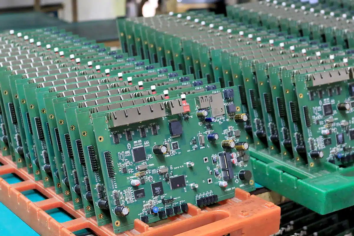
Electronics Manufacturing

by Andrew Williams

The manufacturing labor shortage is a pressing concern for American electronics companies, where the scarcity of long lead-time components is matched by a shortage of skilled workers. Decades of job losses in the manufacturing sector have resulted in a lack of interest in manufacturing careers among potential workers who lack personal connections to the industry. To address this issue, companies are exploring various strategies, such as increased automation and training collaborations with community colleges. They have also found success by offering flexible work schedules that cater to the preferences of college students, single parents, and retirees.

One effective solution for electronics companies seeking to combat labor shortages is to consider populations that have been overlooked in the past, such as people with disabilities. PRIDE Industries, the company where I work as Director of Product Engagement, has been a pioneer in employing individuals with disabilities since its inception in 1966, when it was founded by a group of parents seeking employment for their adult children with disabilities. Today, PRIDE Industries is the leading employer of people with disabilities in the nation. We employ thousands of individuals in our lines of business and have helped thousands more find jobs with other companies.

How Employees with Disabilities Mitigate the Manufacturing Labor Shortage

The line of business in which I work—Manufacturing and Logistics Services (MLS)—was established in the 1990s when one of our customers asked us to manufacture a new product for them. Since this product had a simple production flow, it was well-suited to inexperienced production workers. Starting with a job shop that performed through-hole assembly using a slide line, our division has grown into a comprehensive EMS provider with full SMT capabilities. We now produce a variety of products, including Class II medical devices, using an inclusive workforce that includes a high number of people with disabilities.

It’s a proven fact that employees with disabilities have lower turnover and absenteeism than average.

Head shot of Andy Williams
Andrew Williams, Director of Product Engagement, PRIDE Industries

People with disabilities are one of the most underrepresented groups in the labor force. Two-thirds of working-age Americans with a disability are unemployed, even though many want to work. Given that one in four Americans has a disability, this is a significant waste of talent.  At PRIDE Industries, we’ve successfully created employment opportunities for this labor pool, which enables us to reap the benefits of a broad talent base.

How to Make the Factory Floor More Inclusive

Integrating people with disabilities into the production line requires thoughtful planning. For example, job descriptions sometimes need to be modified to align better with an employee’s specific skill set. And often, new fixtures, tooling, and jigs must be developed to support the integration of employees with disabilities into production roles. But the benefits of these efforts are substantial. Our inclusive workforce demonstrates a level of focus and consistency that surpasses that of the general workforce. And it’s a proven fact that employees with disabilities have lower turnover and absenteeism than average. It’s no surprise, then, that our 30 years of experience have taught us that the benefits of accommodating employees with disabilities more than outweigh the costs.

While hiring people with disabilities may not completely resolve the manufacturing labor shortage faced by electronics manufacturers, it can significantly alleviate talent issues for many organizations. And there are broader societal benefits to recruiting from this underrepresented segment of the labor market. By providing the right opportunities, we can empower individuals with disabilities to become independent. Hiring from this talent pool also addresses chronic unemployment and reduces the underutilization of valuable production resources, a benefit that aligns with lean manufacturing principles.

For over 30 years, PRIDE Industries has proven the value of an inclusive workforce. Employing people with disabilities not only changes lives, but also brings real material advantages to the companies that provide these opportunities—advantages that extend far beyond the obvious ESG benefits. Even the surrounding community benefits, in the form of reduced safety net costs and an increased tax base. When you build an inclusive workforce, it’s a win for your employees, your company, and the community you call home.

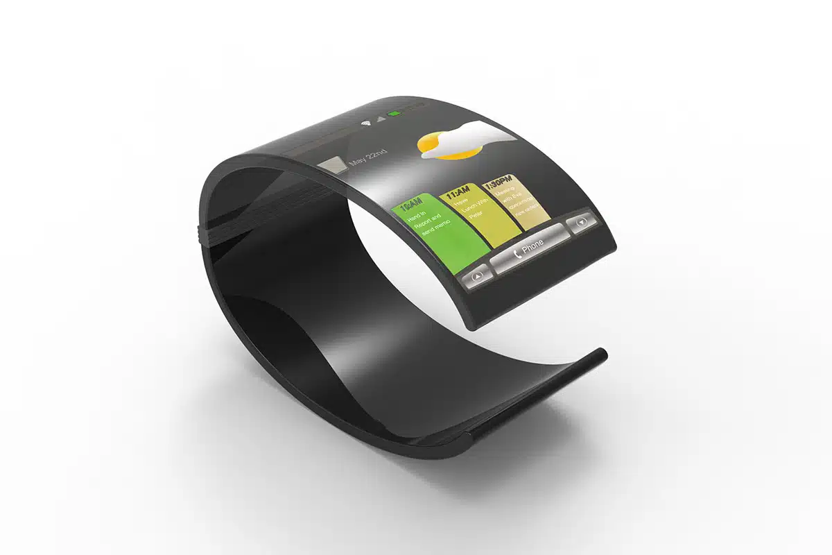
Let’s Talk Business

Looking for a skilled team to produce your next electronics device? Our highly trained, inclusive manufacturing workforce ensures top-notch quality. And our team of SMTA-certified process engineers can help you design, test, and get your product to market fast. Contact us today to learn more.
Have you ever heard the story behind the household cleaner Formula 409®? It’s a tribute to the tenacity of two Detroit-based scientists. It took them 409 attempts until they hit upon a cleaning formula that worked the way they wanted.
The journey of Formula 409®’s inventors is not an anomaly. It took Sir Tom Dyson, inventor of the dual cyclone bagless vacuum cleaner, exactly 5,126 iterations to achieve his desired result. And although the number of iterations a new product goes through can vary significantly—due to design team expertise, the complexity of the product, the industry, etc.—almost all products go through a trial-and-error phase before success is achieved. And all this experimentation can be costly. Fortunately, inventors have an ace up their sleeve: prototyping, and more recently, rapid prototyping.

The efficiencies of rapid prototyping support iterative design and therefore more highly refined components.

What is a Prototype?

A prototype is a draft version of a product or design which allows the creator to test and improve a concept or process before releasing a final version. For example, an inventor might share a prototype with a manufacturer for help in modifying and testing the design. In electronics, one might build an actual version of a theoretical circuit to verify that it works. And if it doesn’t—which at the beginning of the design process, is often the case—the prototype provides a physical platform for debugging.

What is Rapid Prototyping?

Creating a prototype saves time and money; however, traditional prototyping can still be costly and time consuming. Fortunately, manufacturers now have rapid prototyping. As its name implies, rapid prototyping is a way to quickly fabricate a prototype to aid designers in visualizing, redesigning, and developing a product before mass production. Rapid prototyping differs from traditional prototyping in that it emphasizes speed, efficiency, and flexibility.

Rapid prototyping is made possible by new advances in technology, such as the FlexBoard, which was developed by MIT researchers. The FlexBoard is a flexible breadboard that allows rapid prototyping of objects with interactive sensors, actuators, and displays on curved and formable surfaces. Because of the FlexBoard’s design, it allows for more rapidly customizable interfaces.

A man and a woman, standing at a desk in a manufacturing facility, looking at a laptop computer screen.
With rapid prototyping, designers and engineers can immediately update designs based on real-world testing.

Other advanced prototyping technologies include computer-aided design (CAD) and additive manufacturing, more commonly known as 3D printing. Almost all rapid prototyping involves CAD, a technology that relies on a computer to help in the creation, modification, analysis, and optimization of a design. CAD allows for the design and production processes to blend seamlessly, since an electronic output file from the software leads directly to the part production, with changes able to be made at any time during the workflow. 

The auto industry was among the first to embrace rapid prototyping, but other industries were not far behind. Today, electronics manufacturers are creating rapid prototype circuit boards for a wide variety of applications, particularly for products that have no leeway for error—such as defense, medical, aerospace, and robotics devices.

Why is Rapid Prototyping So Important?

The time and effort needed to get a sophisticated electronics product to market is legendary, and the growing complexity of these devices isn’t making it any easier. But a concurrent development is. CAD was one of the first rapid prototyping technologies developed, and it has sped up the development process for new products considerably. Now the addition of a newer technology, 3D printing, is cranking up the speed even more.

And that’s a good thing, because semiconductors—and the devices they enable—are evolving more quickly than ever. Customers now expect significant improvements to existing products on a regular basis. And new products have to dazzle. Rapid prototyping is what makes that possible, by optimizing development and production in seven important ways:

3D printing allows designers to create non-planar electronics with unique form factors.
  • Efficiency: Rapid prototyping techniques provide more efficiency during the R&D process. With traditional prototyping, engineers frequently wait weeks to receive a prototype from a short-run manufacturer—only to discover the need to start again. With rapid prototyping, designers and engineers are now able to produce prototypes in a matter of hours so they can immediately update designs based on test results.
  • Cost-effectiveness: The increased efficiency of rapid prototyping also saves money. With rapid prototyping, companies can test boards and find problems before a production run—saving both material and employee time. Furthermore, rapid prototyping accelerates the testing and verification process, reducing the overall manufacturing and design costs for a project.
  • Better Components: Iterative design is a cyclical methodology for prototyping, testing, analyzing, and refining. This methodology enables manufacturers to produce the best electronic components possible. In the past, it was not always possible to produce an accurate prototype board that allowed designers to determine how best to modify a board layout for optimal performance. The efficiencies of rapid prototyping, however, support iterative design and therefore more highly refined components.
  • Fewer Supply Chain Challenges: Supply chain challenges have affected many industries, including electronics. You can’t create a prototype if you don’t have the materials. Fortunately, additive manufacturing technology provides a simple solution: create it yourself on a 3D printer.
  • Flexibility in Materials: Additive manufacturing systems are more flexible with regards to materials than tools typically used in traditional prototyping. The 3D printers used with rapid prototyping can accommodate a wide variety of materials, such as plastic, powders, resins, metal, and carbon fiber.
  • Flexibility in Design: Designers are no longer limited to creating rigid planar PCBs. Because of its layering properties, 3D printing allows designers to create non-planar electronics with unique form factors, as well as integrate functionality on to a single board. Rapid prototyping also allows testing of complex designs that would otherwise be costly and time-intensive to produce. For example, with a perfboard or a stripboard there are soldering limitations and track destruction challenges that don’t exist with rapid prototyping.
  • Small Batch Runs: With traditional prototyping, it’s often not practical to produce a small batch of PCBs. With rapid prototyping, on the other hand, it’s feasible to produce limited batches of 5 to 100 units.

The Future of Rapid Prototyping for Electronics

Innovative new technologies, such as advancements in CAD and other design tools, will continue to increase the use of rapid prototyping. And as more robust systems and materials for additive manufacturing become available—and more affordable—rapid prototyping of electronics will become more widely adopted and better integrated with traditional manufacturing and assembly steps.

These developments are already well under way. Artificial intelligence (AI), for example, is expanding into multiple disciplines, and the area of rapid prototyping is no exception. As AI improves, it will continue to be integrated into rapid prototype development, with the ultimate goal of more data-driven decisions and seamless testing.

How far can this trend go?

Despite all the advances in CAD, additive manufacturing, and AI, full automation of electronics manufacturing remains a distant goal, according to All About Circuits, one of the world’s largest, independent online communities for electrical engineers. That said, it is certain that strategies like rapid prototyping will continue to move the industry forward and remove previous barriers. As with most developments in electronics manufacturing, the limits of rapid prototyping technologies have yet to be reached.

An Electronics Contract Manufacturing Partner You Can Rely On

Our flexible, customized electronics manufacturing and logistics services are supported by highly skilled staff and driven by a commitment to quality that extends to all the services we offer. From streamlining product designs for greater efficiency, to high-precision manufacturing, to supply chain management, shipping, and recycling services, our team can help you get the most from your product’s entire lifecycle.

In 1957, a researcher named Joseph P. Mammola developed a new technique for PCB assembly that helped usher in second-generation computing: through-hole technology. That technology was the gold standard until the 1980s, when it was largely supplanted by surface-mount technology (SMT), which allows for increased automation of the assembly process. Today, the SMT process is the dominant choice for PCB assembly, offering improved efficiency, cost-effectiveness, and better performance. But to reap these benefits, you need the expertise of certified SMTA engineers.

How can qualified engineers streamline and optimize manufacturing to provide reliable electronic products that customers demand? Here are five essential areas where EMS engineers, qualified in the SMT process, can add a critical edge to the manufacture of your product.

Design for Manufacturability and the SMT Process

Engineers play a vital role in optimizing your product’s circuit board. Even before tooling starts, qualified SMT process engineers can examine and assess design files, including schematic diagrams and assembly drawings, to identify potential issues. Approaching design problems early in the process results in improved manufacturing efficiency and reduced waste.

Getting the most from these reviews means working with SMT engineers who are knowledgeable in design for manufacturability (DFM) and have an extensive background in board design. Design-savvy engineers can evaluate board files and suggest reconfigurations that simplify assembly and replace scarce custom parts with readily available standard ones. These design reviews can also lead to modifications that enhance yield rates and minimize rework at a later stage.

For some electronic devices, a balance has to be struck between DFM best practices and product performance levels. If this is the case, you should be able to count on your EMS engineers and their teams to explain the situation and review options.

Design-savvy engineers can evaluate board files and suggest reconfigurations that simplify assembly and replace scarce custom parts with readily available standard ones.

A woman and a man in glasses seated at a table in a manufacturing facility, examining one of the components of an electronics device.
Reviewing component selection in the design phase can reduce production costs and optimize product performance.

Component Selection and Cost Reduction

Selecting appropriate components is crucial for cost-effective electronic manufacturing. SMT process engineers, who have a deep understanding of electronic components, can provide valuable insights into parts selection.

Before production starts, engineers should review a product’s bill of materials (BOM) and Pick-and-Place (PnP) files to gather important information about component type and placement.

Armed with this information, engineers can select components that will set the foundation for a product’s commercial success. For most devices, it’s best to avoid nonstandard components that require hand-soldering and instead choose readily available parts that can be installed using machine-based processes, ensuring greater consistency and streamlining the assembly process.

Experienced engineers can identify off-the-shelf components that offer custom-part performance at a lower cost. Moreover, working together with your EMS provider’s procurement team, they can evaluate the availability and reliability of components, ensuring long-term sustainability and reducing the risk of supply chain disruptions.

By leveraging the knowledge of SMT process engineers, component selection can be optimized to significantly reduce manufacturing costs without compromising performance or durability.

In addition to selecting the most effective components, SMT process engineers can use the information from PnP files to optimize the placement of these parts on the board, so that the orientation and spacing of microchips and other components meets all manufacturability and testing requirements, delivering the best performance possible.

Design for Testability and Regulatory Compliance

Manufacturing a reliable electronic product cannot be done without thorough and efficient testing. Whether custom or standard, testing the components and configuration of a PCBA is an essential part of the manufacturing process.

For the most efficient testing, SMT process engineers use design for testability (DFT) guidelines that optimize testing during the manufacturing process, ensuring that any potential defects or issues are identified early on. Engineers can strategically place test points, incorporate built-in self-test features, and design for automated testing, all of which contribute to faster and more accurate testing procedures. By catching problems early, significant time and costs associated with diagnosing and rectifying issues during later stages of manufacturing or even post-production can be saved.

In addition to DFT know-how, qualified SMT process engineers can also provide essential guidance during any certification processes, ensuring that products meet safety, electromagnetic compatibility, and other regulatory requirements. This expertise mitigates costly recalls, legal repercussions, and potential damage to a brand’s reputation.

Engineering expertise and a proactive approach to testing and quality assurance minimizes the risk of defects and ensures that only high-quality products reach the market.

Prototyping and Iterative Development

Before mass production, most products benefit greatly from testing and development with the use of small-run prototypes. SMT process engineers who also have expertise in prototyping technologies and methodologies can enhance and accelerate this product development cycle.

By quickly producing functional prototypes, engineers can provide valuable feedback, validate designs, and ensure that necessary improvements are adopted early on. This iterative approach minimizes the risk of expensive errors and redesigns, ultimately reducing time-to-market and ensuring a high-quality end product.

Working with experienced engineers throughout the prototyping and design phase of your product’s development will ensure you get the most out of each design iteration.

End-of-Life Benefits and Sustainability

With sustainability on the mind of many consumers, the lifecycle of electronic products is increasingly under scrutiny.

That’s why it’s more important than ever to work with SMT process engineers who are well-versed in sustainability considerations for electronic products—experts who can consider materials sourcing and end-of-life recycling options during the design phase and find ways to mitigate the negative environmental impact of a product. 

Experienced contract manufacturing engineers enable companies to produce products that have boards with a lower VOC conformal coating and are configured to use less electricity. They can incorporate components which are easily harvested for resale or recycle at the end of the product’s lifecycle. And they can even design products that can be opened up and modified by the end user.

SMT process engineers can configure boards for easy resale or recycling of components at a product’s end of life.

Finding the Right SMT Process Engineers

SMT process engineers don’t just play a key role in a product’s design and development, they can also provide valuable post-production support, such as troubleshooting, failure analysis, and product improvement. And by analyzing field data and customer feedback, they can identify areas for enhancement and implement design updates or manufacturing process refinements. And with supply chains for electronics components still in flux, SMT process engineers are proving invaluable at redesigning existing products whose components are no longer available or in short supply.

So how do you make sure you’re working with experienced engineers?

One way is to make sure the engineers you’re working with are properly certified. The Surface Mount Technology Association (SMTA) offers a certification that can help identify high-caliber talent. Known as the SMTA certification, or the SMT Process Engineer certification, it offers global recognition for engineering expertise.

Working with SMTA-certified engineers means your product manufacturing is being overseen by a distinguished group of only 538 certified engineers worldwide. These highly trained, experienced SMT process engineers have the expertise to ensure that your electronics device is optimized for functionality, quality, and reliability. And they can help you reach these performance goals while minimizing manufacturing costs.

Electronics Manufacturing Expertise that You Can Rely On

At PRIDE Industries, our flexible and customized electronics manufacturing and logistics services are supported by highly skilled, SMTA-certified engineers and driven by an unwavering commitment to quality. From streamlining product designs for greater efficiency to high-precision manufacturing and end-of-life product management, our experienced staff can help you achieve all your manufacturing goals.

From concept to consumer, there’s a lot involved in bringing an electronic product to market. At every stage—design, development, prototyping, production, and manufacture—careful planning is the key to success. This is why it’s essential to carefully plan out your fixture design for manufacturing and testing. Well-designed fixtures ensure reliable and streamlined production processes and ultimate customer satisfaction. And this is especially true when it comes to test fixtures.

Why Focus on Fixture Design for Electronic Manufacturing?

Fixtures enable consistent and repeatable positioning of components, allowing programmed tasks to be performed with precision and accuracy, and mitigating the possibility of bottlenecks in production. When your device is ready to be produced at volume, having the fixture designs already mapped out will mean higher efficiency and throughput.

From large medical or aerospace products, to small consumer electronics, every industry relies on testing to ensure quality and reliability.

For best results, fixture design for electronic manufacturing and testing requires the engineering and design skills of a professional engineering team that’s well-versed in both DFM (Design for Manufacturability) and DFT (Design for Testability) principles. These professionals will ensure that fixtures are designed and positioned for easy testing and optimal production efficiency.

Test Fixtures: Know the Objectives, Plan the Parameters

Achieving optimum results from any test fixture will require working with a qualified electronic manufacturing services (EMS) provider to plan the test fixture’s design with the specifications of the DUT (device under test) in mind—in addition to volume, turnaround, and budget considerations. While customization and planning may add time and some initial cost to the manufacturing process, this is offset by net time saving and cost reduction per item.

Test objectives, determined by industry standards, and the product’s final use and destination will define which test parameters should be incorporated into test fixtures and testing procedures. The test fixture customization and design are planned using CAD systems and software that set test points, calibration, and the collection of data specific to your product. Whatever level of testing you would like to perform, it’s important to consult with your EMS provider regarding the basic inspection requirements your device must satisfy.

Since determination of the fixture design will depend on the functionality and complexity of your device, there are cases where a simple test fixture with few test points and minimum customization—or even an “out of the box” fixture—will be sufficient. In other cases, a more complex test fixture—one that has to be precisely positioned and aligned—may be required.

The selection and deployment of test fixtures will also depend on factors such as production volume, size of the product, and desired quality standards, as well as the overall flow of the assembly process. Costs will also vary depending on the complexity of each fixture and the number of test points that are required. In general, simple test fixtures are less expensive than complex test fixtures.

A pair of engineers inspecting a prototype, with a large schematic on a display screen behind them
Testing can provide data specific to your device that can aid in its refinement.

Test fixtures will not eliminate test failures, as any manufacturing process has an inherent failure rate. However, tests designed with the help of skilled SMT engineers will catch faults early and minimize failure rates.

What Are the Benefits?

Although test fixtures for different devices and products will vary in the type and number of tests required, the overarching benefits of fixture design for electronic manufacturing are consistent:

Time and Cost Savings: Test fixtures streamline the testing process by automating test procedures and identifying defects early in the manufacturing process. With this fast and efficient testing, productivity is increased, and manufacturing cycle time reduced. Test fixtures contribute to cost savings by preventing component misalignments, minimizing scrap rates, and avoiding costly rework.

High Quality Control: When a PCB fails a test, a test fixture can help isolate the specific component, connection, or circuit responsible for the failure. This facilitates troubleshooting and debugging, enabling engineers to identify and rectify issues efficiently, improving the overall manufacturing yield and product quality.

Well-designed, automated testing can reduce the number of steps in your manufacturing cycle.

Consistent Test Methodology: Designed with precise parameters for your product, fixtures enforce a standardized test methodology across the manufacturing process and provide consistent and repeatable test conditions for devices. This promotes uniformity in performance, making it easier to identify and address any anomalies or deviations from the expected results.

Compliance with Standards and Regulations: With the final product in mind, fixtures can be designed to adhere to industry standards, safety regulations, and specific certification requirements. They help ensure that PCBs and devices meet the necessary compliance criteria, providing confidence in the reliability and safety of the electronic device.

What Test Fixtures Should You Use?

Your engineering team, working with your EMS provider, will have the best insights and expertise in determining which tests will be beneficial for your product. Here are some of the test systems that may be considered:

ICT (In-Circuit Test): This is a test system predesigned with a fixed probe layout that matches the layout of the circuit board. The benefit of the ICT test fixture is that by probing individual components and connections on densely populated circuit boards, it produces very detailed test data. It typically uses a bed-of-nails or pogo pin configuration to make contact with test points on the board.

FCT (Functional Circuit Test): This fixture test does not test single components but instead tests the overall functionality of the assembly or the function of assembly networks. A functional test fixture will evaluate the powered-on state and replicate the end application and expected functions. The test is generally conducted at the end of assembly and is helpful in product debugging and development.

Boundary Scan: Boundary scan testing, as defined by the IEEE 1149.1 standard, is primarily designed for JTAG-compatible devices. The boundary scan chain is a set of test points that are located on the edges of the PCB that can be used to test the connections between the components on the board. As a test defined by the IEEE standard, it has the advantage of ensuring consistency and compatibility across devices. The test also addresses the physical space constraints of denser boards and the loss of physical access to signals.

Environmental tests: Environmental test fixtures are used to test the PCB’s performance under the environmental conditions it’s going to be used in. This testing can be used to test the PCB’s resistance to temperature, humidity, vibration, and other environmental factors.

Burn-In Test: A burn-in test is used to detect early component failure, which is why it’s especially critical for medical or military devices. Burn-in testing involves subjecting electronic devices or components to extreme stress conditions. This usually involves running the board for 48 to 168 hours to ensure long-term reliability. A burn-in test fixture provides the necessary environment and connections for performing these tests.

Getting the Most from Fixture Design for Electronic Manufacturing

From large medical or aerospace products, to small consumer electronics, every industry relies on testing to ensure quality and reliability. Without adequate and consistent testing consumers will experience inferior products and lose confidence in the electronic devices they depend on.

No matter what tests are determined to be the best for your product, the best results will come from planning ahead with input from engineers skilled in DFM and DFT. Designing test fixtures into your assembly line will mean fewer returns and greater customer satisfaction. Customers will never see it, but they will definitely appreciate it.

An Electronics Manufacturing Partner You Can Rely On

PRIDE Industries offers flexible, customized electronics manufacturing and logistics services, supported by highly skilled staff and driven by a commitment to quality. Our experienced engineers can ensure you meet all your manufacturing goals, from optimal test fixture design to end-of-life recycling.
Centuries ago, the invention of paper led to the development of a new art form—origami. As the art form spread, practitioners learned to manipulate a single sheet of paper into ever-more complex figures. Even in recent years, new fold techniques have been developed by masters of the art. Some of these new techniques—along with more traditional ones—are now being applied in a way that the inventors of origami could never have imagined. This ancient art, once practiced by monks and nobles, is now making possible the next generation of electronic devices.

Origami techniques enable versatile three-dimensional (3D) structures to be created from planar, two-dimensional (2D) sheets. The versatility made possible by these techniques means that origami has potential applications across a wide range of industries, including space exploration, electronics manufacturing, robotics, and medicine.

Why Use Origami for Electronic Devices?

Origami fold patterns can add structural integrity to an object, as well as affect its mechanical and metamaterial properties.

By creating a 3D object out of a 2D piece of paper, origami provides unique structural solutions to many engineering problems.

Origami fold patterns can add structural integrity to an object, as well as affect its mechanical and metamaterial properties. The Miura fold (a fold conceived in 1970 by astrophysicist Koryo Miura), for example, can confer both rigidity and compressibility to a non-rigid material. Using techniques like the Miura fold, engineers have made lightweight, foldable robotic parts that weigh only 30 grams, yet can unfold and self-lock to become rigid and capable of sustaining a compressive load of 12 kilograms.

Saving Space—in Space

As with many fabrication and engineering innovations in the field of electronics manufacturing, some of the first technological applications for origami were in space.

Using origami provides aerospace engineers with an elegant way to construct complex structures that can fold down for easy (and less expensive) transport. Then, once the devices have reached orbit, they can seamlessly open up to several times their size. And if needed, they can return to their folded state just as easily as they unfurled.

Origami has already been successfully used by NASA and other space programs to design large objects that are lighter in weight than their traditional counterparts, and smaller too, so that they significantly reduce the volume taken up in the spacecraft.

In fact, the recent launch of the largest telescope ever into space—the James Webb Space Telescope—was made possible by the use of techniques borrowed from origami and its related discipline, kirigami. Both the mirror and the giant sunshield, 21 feet and 69.5 feet respectively, folded down to fit into a narrow 18-foot rocket opening.

By enabling the creation of new types of electronic devices, origami is also creating new areas of demand for electronic components. The mirror of the Webb telescope, for example, was unfolded with the aid of miniaturized SIDECAR microprocessors. These processors, designed to convert analog to digital signals, had been miniaturized from a volume of about one cubic meter to an integrated circuit about the size of a half-dollar coin—demonstrating how innovation in one area often pushes development in another.

Making Electronic Devices Less Expensive and More Sustainable

With precise folding, manufacturers can also produce more complex and intricate designs without the stress development issues associated with traditional designs.

The Ohio-based company, Industrial Origami, specializes in the low-force folding of steel and aluminum sheets. The company has patented a technology that uses origami principles to simplify the design and assembly of a host of products, including heavy construction goods. According to the company, their origami-based designs reduce material usage by 20 to 50 percent, while making the production process easier, faster, and less expensive.

Two people in a living room, using their wall-mounted smart home interface
Origami is set to create greater efficiency in sensory technology.

Another company that has taken space-saving folding techniques to the factory floor is the Swedish company Stilride. Using “industrial origami” techniques, the company is able to build an e-bike out of a single sheet of stainless steel. Bicycles made this way are more sustainable than traditionally made bikes, because they use fewer raw materials. They’re also 40% lighter and cost 20% less to build.

Not only is this origami folding technology scalable, it also allows for a flexible manufacturing model where lightweight, flat modules can be easily transported elsewhere for assembly.

Shifting Shapes

Engineers are looking to origami techniques to create shapeshifting, reconfigurable structures, particularly in the development of antennas and antenna arrays.

Origami accordion designs, for example, enable the construction of highly flexible antennae. These bendable antennae are capable of movement beyond a single linear functionality, which gives them the ability to work at two different frequencies.

In another novel application of origami, engineers at Princeton University have been working on antenna arrays using a new class of broadband metasurface antenna. These antennas are arrayed in a configuration that’s based on an origami pattern for a folded paper box called a waterbomb. This highly flexible waterbomb array confers much higher functionality than the standard antenna array, enabling the careful calibration of electromagnetic waves.

As demand grows for robotics, smart devices, and other wireless-dependent technologies, robust and flexible antenna arrays will become more critical. Sensing antennas are already low-cost and lightweight. Now, origami-inspired arrays are making them more useful and easier to deploy on a wide scale.

Flexible Semiconductors for Flexible Devices

As wearables, soft robots, and other flexible electronics grow in popularity, origami has found its way into the design of semiconductors.

Flexible electronic devices require materials and designs that mitigate the strain and movement that produces unwanted electronic signals. PCBs and their components—especially semiconductors—are becoming more flexible, and origami is inspiring new PCB and device designs that take advantage of this pliability.

To this end, engineers at the University of Illinois at Urbana-Champaign are using kirigami—origami’s sister technique that uses cutting in addition to folding—to produce elastic-like semiconductors that won’t cause troublesome signal outputs. These designs use atomically thin graphene sandwiched between two layers of polyimide to create a highly flexible material, which is then engineered using a kirigami design to further enhance stretchability. These novel semiconductors have proven to be highly strain tolerant and function without producing unwanted motion or signals.

Nanomaterials like graphene are contributing to the next generation of microchips.

In another area of strain engineering (aka “straintronics”), researchers at the University of Sussex have been working with graphene and other 2D nanomaterials to create transistors by using a folding process called “nano origami.” With nano origami, kinks and folds are made in a 2D sheet of graphene—which is itself composed of only a single layer of carbon atoms—to create the smallest ever microchips. These graphene microchips, still in development, will be 100 times smaller than regular microchips. By enabling electronics manufacturers to add dozens of chips to devices without increasing their size or weight, these extremely small microchips seem poised to usher in a new era of electronics.

Self-Assembling Packaging

Perhaps the most obvious application of origami (and kirigami) is in an area that relies heavily on paper and paper-like materials—packaging. With hard plastic losing favor as a packaging material, and with paper and other flexible, organic substances growing in popularity as sustainable substitutes, it’s no surprise that origami is playing an increasingly important role in packaging design.  

One of the most innovative developments in this area is the creation of self-folding packaging, which is adding an efficient new twist to a traditional packaging design—the honeycomb.

Honeycomb structures have all the right properties for good packaging: low weight, effective heat insulation, and high shock absorption. But the folding process has traditionally been time-consuming and impractical, especially for very large or small objects.

That may be changing, however. A group of Japanese scientists have created a packaging design that combines dry paper with wet ink to create a packaging material that folds itself into a honeycomb shape—without mechanical intervention. Best of all, the material can be easily replicated, because what makes this packaging unique isn’t the raw material used to make it, but the pattern of the ink coating that’s applied to the paper.

With this process, low-cost paper is run through an ink-jet printer to coat it with a pre-designed pattern of printing solution. Once the paper comes off the printer, it self-assembles into the desired shape—ready to fit objects of any size.

This yields a sustainable packaging solution that can provide snug cushioning for small or fragile products and absorb shocks and impacts for large unwieldly structures, reducing the risk of damage during transportation.

Future Prospects for Ancient Techniques

From giant telescope mirrors to nano-folded microchips, the art of origami applied to industrial design is set to create more efficient and sustainable products that are cheaper to produce and easier to transport. And with origami techniques just beginning to be utilized for electronics, there are likely many more useful applications for this ancient art that are yet to be discovered.

Electronics Design and Manufacturing Services

Our flexible, customized electronics manufacturing is supported by highly skilled engineers and driven by a commitment to quality and exceptional customer service. From streamlining product designs for greater efficiency, to high-precision manufacturing, to end-of-life product management, our team can help you get the most from your product’s lifecycle.